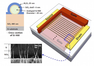
Si-nanowire (Si-NW) based thin-film transistors (TFTs) have been considered as a promising candidate for next-generation flexible and wearable electronics as well as sensor applications with high performance. Here, we have fabricated ambipolar Schottky-barrier (SB) TFTs consisting of a parallel array of Si-NWs and performed an in-depth study related to their electrical performance and operation mechanism through several electrical parameters extracted from the channel length scaling based method. Especially, the newly suggested current-voltage (I-V) contour map clearly elucidates the unique operation mechanism of the ambipolar SB-TFTs, governed by Schottky-junction between NiSi2 and Si-NW. Further, it reveals for the first-time in Schottky based FETs the important internal electrostatic coupling between the channel and externally applied voltages. This work provides helpful information for the realization of practical circuits with ambipolar SB-TFTs that can be transferred to different substrate technologies and applications.

Si-nanowire (Si-NW) based thin-film transistors (TFTs) have been considered as a promising candidate for next-generation flexible and wearable electronics as well as sensor applications with high performance. Here, we have fabricated ambipolar Schottky-barrier (SB) TFTs consisting of a parallel array of Si-NWs and performed an in-depth study related to their electrical performance and operation mechanism through several electrical parameters extracted from the channel length scaling based method. Especially, the newly suggested current-voltage (I-V) contour map clearly elucidates the unique operation mechanism of the ambipolar SB-TFTs, governed by Schottky-junction between NiSi2 and Si-NW. Further, it reveals for the first-time in Schottky based FETs the important internal electrostatic coupling between the channel and externally applied voltages. This work provides helpful information for the realization of practical circuits with ambipolar SB-TFTs that can be transferred to different substrate technologies and applications.