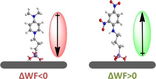
The ability to tune the electronic properties of oxide-bearing semiconductors such as Si/SiO2 or transparent metal oxides such as indium-tin oxide (ITO) is of great importance in both electronic and optoelectronic device applications. In this work, we describe a process that was conducted on n-type Si/SiO2 and ITO to induce changes in the substrate work function (WF). The substrates were modified by a two-step synthesis comprising a covalent attachment of coupling agents monolayer followed by in situ anchoring reactions of polarizable chromophores. The coupling agents and chromophores were chosen with opposite dipole orientations, which enabled the tunability of the substrates WF. In the first step, two coupling agents with opposite molecular dipole were assembled. The coupling agent with a negative dipole induced a decrease in WF of modified substrates, while the coupling agent with a positive dipole produced an increase in WFs of both ITO and Si substrates. The second modification step consisted of in situ anchoring reaction of polarizable chromophores with opposite dipoles to the coupling layer. This modification led to an additional change in the WFs of both Si/SiO2 and ITO substrates. The WF was measured by contact potential difference and modeled by density functional theory-based theoretical calculations of the WF for each of the assembly steps. A good fit was obtained between the calculated and experimental trends. This ability to design and tune the WF of ITO substrates was implemented in an organic electronic device with improved I-V characteristics in comparison to a bare ITO-based device.

The ability to tune the electronic properties of oxide-bearing semiconductors such as Si/SiO2 or transparent metal oxides such as indium-tin oxide (ITO) is of great importance in both electronic and optoelectronic device applications. In this work, we describe a process that was conducted on n-type Si/SiO2 and ITO to induce changes in the substrate work function (WF). The substrates were modified by a two-step synthesis comprising a covalent attachment of coupling agents monolayer followed by in situ anchoring reactions of polarizable chromophores. The coupling agents and chromophores were chosen with opposite dipole orientations, which enabled the tunability of the substrates WF. In the first step, two coupling agents with opposite molecular dipole were assembled. The coupling agent with a negative dipole induced a decrease in WF of modified substrates, while the coupling agent with a positive dipole produced an increase in WFs of both ITO and Si substrates. The second modification step consisted of in situ anchoring reaction of polarizable chromophores with opposite dipoles to the coupling layer. This modification led to an additional change in the WFs of both Si/SiO2 and ITO substrates. The WF was measured by contact potential difference and modeled by density functional theory-based theoretical calculations of the WF for each of the assembly steps. A good fit was obtained between the calculated and experimental trends. This ability to design and tune the WF of ITO substrates was implemented in an organic electronic device with improved I-V characteristics in comparison to a bare ITO-based device.
