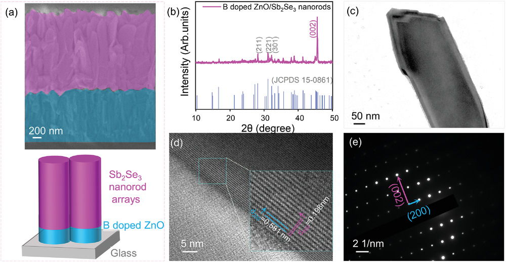
Antimony selenide (Sb2Se3) has garnered significant attention with its extraordinary optical and optoelectronic properties for optical and optoelectronic devices such as broadband photodetectors. The trends emerge in the synthesis of Sb2Se3 over a semiconducting substrate for the direct formation of heterostructures, which facilitate a pn junction for self-powered photodetector. 1D Sb2Se3 nanorods are preferred to boost the charge carrier transport along the longitudinal direction as well as the optical absorption by light trapping. Great challenges remain for the vertical growth of nanorods. In this work, the precisely vertical alignment of Sb2Se3 nanorod arrays has been achieved in an epitaxial growth manner by selecting a lattice-matching substrate, namely, boron-doped ZnO (110) surface. The directly grown boron-doped ZnO/Sb2Se3 nanorod arrays heterostructure leads to a high-performance broadband photodetector. Eventually, the device demonstrates extraordinary figure-of-merit parameters, i.e., responsivity, on/off ratio, and specific detectivity. Furthermore, device simulation predicts the theoretical limit of the photodetector performances on the condition of suppressed defect density of the Sb2Se3. These results may shed light on the investigation of controlled growth of low-dimensional materials, self-powered photodetectors, and related optic and optoelectronic devices.

Antimony selenide (Sb2Se3) has garnered significant attention with its extraordinary optical and optoelectronic properties for optical and optoelectronic devices such as broadband photodetectors. The trends emerge in the synthesis of Sb2Se3 over a semiconducting substrate for the direct formation of heterostructures, which facilitate a pn junction for self-powered photodetector. 1D Sb2Se3 nanorods are preferred to boost the charge carrier transport along the longitudinal direction as well as the optical absorption by light trapping. Great challenges remain for the vertical growth of nanorods. In this work, the precisely vertical alignment of Sb2Se3 nanorod arrays has been achieved in an epitaxial growth manner by selecting a lattice-matching substrate, namely, boron-doped ZnO (110) surface. The directly grown boron-doped ZnO/Sb2Se3 nanorod arrays heterostructure leads to a high-performance broadband photodetector. Eventually, the device demonstrates extraordinary figure-of-merit parameters, i.e., responsivity, on/off ratio, and specific detectivity. Furthermore, device simulation predicts the theoretical limit of the photodetector performances on the condition of suppressed defect density of the Sb2Se3. These results may shed light on the investigation of controlled growth of low-dimensional materials, self-powered photodetectors, and related optic and optoelectronic devices.