Short Description:
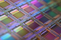
Employing photons in the functional processing components is crucial to improving the data transmission rate and processing speed since the technology of electron-based integrated circuits and electronic devices is quickly approaching its fundamental limits. One of the main elements of a photonic circuit is waveguides, and coupling light into them via integrating a versatile optical source is profoundly desirable. Microlasers are the most reliable option that can generate coherent radiation and perform single-mode photon emission within a tiny footprint. Several optical feedback configurations, such as distributed feedback (DFB), Fabry-Perot cavity, and whispering gallery mode (WGM) lasers, have been fabricated using colloidal semiconductor nanocrystals as the optical gain medium. When using NCs as the gain material, the packing density becomes a crucial factor since the refractive index and the gain coefficient of the final layer are significantly affected by this parameter. Well-defined nanopatterns of colloidal NCs with high-density and close-packed structures can reach high gain values results in superior optical mode confinement. This project focused on fabricating a self-resonant microlaser based on a closed-packed micropattern of 2D semiconductor nanoplatelets.
Tasks:
Details will be announced soon.
Requirements:
We are looking for a top-level student in Materials Science or Natural Science with excellent verbal and written communication skills in English who wants to make a mark in science. Knowledge of working with colloidal semiconductor nanocrystals is an advantage. The candidate must be able to work independently and progress in the research work by own achievements. He/she must be creative in solving experimental challenges. A fundamental part of the work will be reporting the results. The candidate must be experienced in writing technical/scientific reports. It is expected that the candidate has a solid research-ethical approach. The primary workplace will be the Institute of Materials Science and Nanotechnology and Max Bergmann Center of Biomaterials Dresden.
Our group does not discriminate based on race, color, gender identity, religion, or national origin. The application from students with disabilities will be particularly welcome.
Benefits:
We offer exciting tasks in a robust international academic environment as well as an open and inclusive work environment with dedicated colleagues. The student will learn advanced nanofabrication techniques and experience multidisciplinary nanomaterial research and development.
Short Description:
Employing photons in the functional processing components is crucial to improving the data transmission rate and processing speed since the technology of electron-based integrated circuits and electronic devices is quickly approaching its fundamental limits. One of the main elements of a photonic circuit is waveguides, and coupling light into them via integrating a versatile optical source is profoundly desirable. Microlasers are the most reliable option that can generate coherent radiation and perform single-mode photon emission within a tiny footprint. Several optical feedback configurations, such as distributed feedback (DFB), Fabry-Perot cavity, and whispering gallery mode (WGM) lasers, have been fabricated using colloidal semiconductor nanocrystals as the optical gain medium. When using NCs as the gain material, the packing density becomes a crucial factor since the refractive index and the gain coefficient of the final layer are significantly affected by this parameter. Well-defined nanopatterns of colloidal NCs with high-density and close-packed structures can reach high gain values results in superior optical mode confinement. This project focused on fabricating a self-resonant microlaser based on a closed-packed micropattern of 2D semiconductor nanoplatelets.
Tasks:
Details will be announced soon.
Requirements:
We are looking for a top-level student in Materials Science or Natural Science with excellent verbal and written communication skills in English who wants to make a mark in science. Knowledge of working with colloidal semiconductor nanocrystals is an advantage. The candidate must be able to work independently and progress in the research work by own achievements. He/she must be creative in solving experimental challenges. A fundamental part of the work will be reporting the results. The candidate must be experienced in writing technical/scientific reports. It is expected that the candidate has a solid research-ethical approach. The primary workplace will be the Institute of Materials Science and Nanotechnology and Max Bergmann Center of Biomaterials Dresden.
Our group does not discriminate based on race, color, gender identity, religion, or national origin. The application from students with disabilities will be particularly welcome.
Benefits:
We offer exciting tasks in a robust international academic environment as well as an open and inclusive work environment with dedicated colleagues. The student will learn advanced nanofabrication techniques and experience multidisciplinary nanomaterial research and development.